
Semiconductor chips may be the smallest manmade object in human history. The smallest production size of 2 nanometers matches the scale of human DNA. By the end of 2026, Taiwan will have five fabs capable of mass-producing 2nm chips, setting it apart from any other country. It is commonly believed that Taiwan’s chip manufacturing is the product of immense R&D investment and gigafabs. However, this view overlooks Taiwan’s 40-year spatial transformation, spearheaded by Taiwan Semiconductor Manufacturing Company (TSMC, 台灣積體電路製造公司). Indeed, in order to manufacture the world’s most advanced chips, the Taiwanese have had to design not just gigafabs, but also entire cities—and perhaps, their whole nation.
Take, for example, extreme ultraviolet (EUV) machines that employ lasers to produce cutting-edge microchips. Each EUV machine is the same size as a double-decker bus, and a single gigafab will install more than 60 to 80 of these machines. A Gigafab comprises a continuous cleanroom crisscrossed by skyway tracks delivering parts. Under the cleanroom is the sub-fab, housing mechanical, electrical, and plumbing (MEP) systems supporting the cleanroom. The sub-fab is double the size of the cleanroom itself. These dynamics contribute to the enormous scale of modern gigafabs.
Surrounding infrastructure presents an another challenge. Cutting-edge chips are time-sensitive products, and must be shipped to end customers as soon as possible. Robust transportation and logistics systems are therefore crucial to a given country’s chip manufacturing industry. Hence Taiwan’s chip fabs operate along a single transportation line running north to south on the island, connected to numerous ports and air cargo gateways. The global semiconductor industry is a cross-border operation, and Taiwan functions as a one-stop shop cluster that dominates the middle and end of the supply chain. Decades of infrastructure investments from the Taiwanese government have allowed TSMC to push its manufacturing to the limits. This process has created the single most efficient production city-island in the world.
How Industrial Planning and Transportation Made Taiwan a Powerhouse
Before TSMC transformed Taiwan into a global technology titan, the Taiwanese economy was highly reliant on a mix of light, labor-intensive manufacturing and state-backed heavy industries. During the 1970s and 1980s, multiple export processing zones (EPZs) were founded across Taiwan—combining industrial parks with free trade zones. For a city like Kaohsiung, the EPZ and petrochemical industries have shaped the entire cityscape. Whether visiting by rail or sea, a visitor would encounter a smoky, bustling harbor city that powered one of the fastest industrial expansions in modern history.
In this phase of industrialization, Taiwan was divided into different areas according to economic function. Taipei served as the administrative and financial center, while power plants and factories with large land footprints were deployed to surrounding cities. Alongside a population boom and rapid urbanization, Taiwan’s economic growth surged. It was also at this time that SMEs began to thrive and became the backbone of the Taiwanese economy.
From the longitudinal railway line (running from Keelung in the north to Pingtung in the south) and national highway system to the later completion of high speed rail (高鐵) in 2007, the major north-south transportation avenues not only changed Taiwan’s landscape but collapsed its entire western corridor into a single macro-metropolis. It was a modern revolution of time and space, enabling humans and supply chain to effortlessly flow across the island, thus establishing a vital lifeline for the fast-paced semiconductor industry.
As early as the 1970s, Taiwan realized that its labor-intensive industries, such as textiles manufacturing, could no longer guarantee growth in a rapidly developing world. In order to develop high-tech industries, the government founded the Industrial Technology Research Institute (ITRI, 工業技術硏究院), an applied R&D organization based in Hsinchu. In the 1980s, ITRI then empowered its director, Dr. Morris Chang (張忠謀), to develop a next-generation industrial plan. Chang himself founded TSMC in 1987, in Taiwan’s first Science Park (科學園區) in Hsinchu. Indeed, the Hsinchu Science Park was the physical outcome of a study on the successes of Silicon Valley. Today, there are three main Science Parks: in northern, central, and southern Taiwan. The Science Parks form nodes in the island’s “Western tech corridor ” (西部科技廊帶) connected by several transportation arteries.
Today, Science Parks serve as spatial tools through which Taiwan has concentrated its infrastructure, talent, and production. TSMC plays the decisive role in planning. Its massive capital expenditure allows it to shape the development of Science Parks according to its needs. Its R&D center is currently located in the original Hsinchu Science Park in the north—which is also close to the geopolitical and policymaking center of Taipei. Meanwhile, it has scaled up production capacity in southern Taiwan through multi-billion-dollar investments. TSMC’s strategic planning has rendered southern Taiwan—including cities such as Chiayi and Tainan—into a “mega-cluster” for sub-2nm chip production and chip-on-wafer-on-substrate (CoWoS) packaging development.
How a Facility Shapes a City: TSMC’s Fab 18 as an Example
TSMC Fab 18, located in the Southern Taiwan Science Park (STSP) in Tainan, is arguably the single most critical piece of industrial infrastructure on Earth. This is not just because of its massive financial value—the total investment in Fab 18 exceeds NTD 1.86 trillion (USD 57 billion) and the 3nm technology it produces may generate USD 1.5 trillion in half a decade. Rather, the physical scale of Fab 18 and associated infrastructure has shaped the landscape of southern Taiwan. TSMC broke ground on construction of Fab 18 in 2018. Commercial volume production at the fab began in early 2020 with the first wave of 5nm chips. Fab 18 combines a total of eight production phases for both the 5nm and 3nm chips, with a total site area sitting at nearly 100 hectares. The production phases employ an interconnected cleanroom with an automated skyway allowing silicon wafers to be transferred efficiently.
Gigafabs like Fab 18 resemble “vertical sandwiches,” featuring layers of engineering spaces. The cleanroom in the middle is the most important space, and features the highest concentrations of ASML extreme ultraviolet (EUV) lithography machines in the world. The cleanroom accounts for around 20-25 percent of total floor space. Beneath the cleanroom floor sits the massive sub-fab (containing MEP systems) that represents the biggest single functional space in the gigafab architecture. Counting the various floor layers together—including the cleanroom, sub-fab, and others—the total interior square footage reaches 410,669 square meters (about 77 American football fields).
The massive scale of Fab 18 results in a high demand for water and electricity, and has challenged the infrastructure of the host city of Tainan—particularly since the Southern Taiwan Science Park is located in an agricultural area. Rather than letting Fab 18 drain freshwater from local reservoirs, developers built a water reclamation network for the Science Park, and a wastewater treatment center is located next to Fab 18. The water management system allows Fab 18 to essentially use each drop of water 3.5 times before disposal. In response to rising energy demands, the city of Taiwan has accelerated renewable energy development, especially in solar energy.
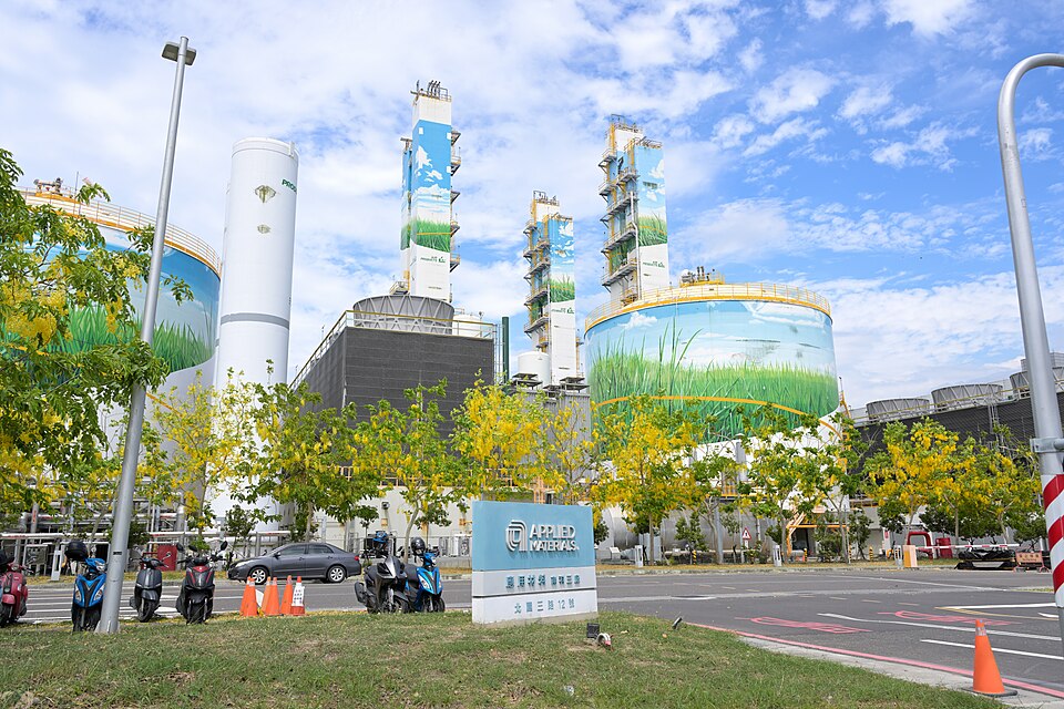
Image: A building complex in the Southern Taiwan Science Park in Tainan (May 2025). (Image source: Wikimedia Commons)
Fab 18 is estimated to employ 14,000 workers. The site does not just create jobs but also spatial effects. It has boosted real estate values in nearby towns like Xinshi, Shanhua, and Anding, and also spawned a massive commuter corridor stretching from the site to Tainan City center and beyond. The Tainan local government has not only sought to expand major roadways but also build public transit, since most commuters rely on scooters and private cars. Commuter trends create an idiosyncratic culture. Entry-level engineers will buy a house in nearby towns because they must frequently respond to sudden call-ups when problems arise, and senior professionals will move closer to downtown Tainan where they can maintain families or more stable lifestyles—yet they must also commute further for work.
Beyond fabs, the semiconductor industry has noticeably shaped logistical infrastructure in Taiwan. Because cutting-edge semiconductors must reach customers quickly or else snag manufacturing lines, upgrades have been essential. Since the 1990s, Taiwan has maintained a goal of becoming the Asia-Pacific region’s operations center. Because of AI-driven demand for Taiwan’s chips, air transshipment centers have appeared at Taoyuan International Airport. The airport will complete its Terminal 3 in 2027, and a new runway is slated for operation in 2032. The new infrastructure will accommodate more advanced logistics centers within the airport’s free trade zone. The Taoyuan airport expansion illustrates a “virtuous cycle” wherein expanding semiconductor exports fosters more advanced logistical infrastructure—which in turns allows for greater exports.
Balancing Efficiency and Livability
Over the past century of rapid spatial modernization, Taiwan has transformed from an agrarian society into a silicon manufacturing hub. While this evolution has generated massive fortunes for those involved, and established a foundation for national security, it has also left undeniably negative effects on Taiwan’s lived environment. Many employees work non-stop inside monolithic, isolated industrial compounds. Although planners have made improvements through architectural and landscape design—such as next-generation “green fabs” that will aim not just for carbon capture but also healthier working conditions—these measures cannot counter the reality that life inside Taiwan’s Science Parks is deeply dichotomous: split between a rigid, grid-like campus and an organic, sometimes chaotic urban environment.
Italian architecture theorist Aldo Rossi said: “The city is the biggest man-made object in the world.” To Rossi, the city was not a random collection of buildings or a passive backdrop to economic activities. Through this lens, Taiwan has successfully transformed itself into a highly efficient and unified man-made artifact. The west coast of Taiwan is one of the most important tech corridors in the world, and this “macro-city” has been designed to process silicon at a global scale, far beyond people’s imagination. Yet there remains another layer in this landscape transformation process: memory. At the center of Southern Taiwan Science Park is a grand building clad in stone. It is the Museum of Prehistory, dedicated for the artifacts discovered by construction teams when the Science Park was built. This chiseled, onyx structure reminds us that this silicon island still wants to be remembered for other things, besides just industrial efficiency.
Conclusion
Over decades of continuous infrastructural investment, Taiwan has harnessed spatial organization in order to compete in global trade. When conceptualizing Taiwan’s comparative advantages in semiconductors, take note that the island’s strengths are not only technological—they are geographical, institutional, and infrastructural. That is what makes Taiwan’s experience in spatial management valuable to other countries.
Indeed, the key lesson Taiwan can provide spatial planners is not its specific orientation of transport networks or Science Parks, but rather how it has adapted rather disadvantageous territory to support its semiconductor industry. Taiwan is a narrow island divided by mountains, yet it has adjusted to this geography by constructing a north-south corridor connecting all of its manufacturing and trade infrastructure. For policymakers, Taiwan’s lesson in spatial management is the requirement to understand one’s geographical canvas and to bridge local nodes and the global supply chain.
Policymakers should be aware that different locations confer their own advantages. For instance, in the emerging semiconductor cluster in less-populated Arizona, a high-volume transportation system can be planned when developers first come in. Early planning would greatly enhance future standards of living. And in Kumamoto, where TSMC jointly operates another fab, how the facility productively complements the city’s legacy industry cluster will be another important consideration.
As other countries seek partnerships with TSMC to cultivate native semiconductor industries, they will inevitably ask the planning questions that have preoccupied Taiwan for decades. Therefore, Taiwan is not only exporting semiconductor manufacturing, but an entire model of spatial organization.
The main point: Taiwan’s semiconductor success is not just a result of technology or capital investment, but the outcome of decades of continuous spatial transformation. By integrating Science Parks and advanced gigafabs across its western transport corridor, Taiwan has become a hyper-efficient, island-sized production system. As TSMC expands globally, Taiwan is exporting not only chip manufacturing, but an entire model of spatial organization.